01 / Context
Overview
The project develops a scalable series-parallel active switched-inductor DC-DC step-up converter for high conversion-ratio applications. The design target is approximately 40 V to 400 V at the kilowatt scale, with the topology, semiconductor stresses, passive components, PCB layout, and feedback control treated as one integrated design problem.
In addition to the power stage, the work includes small-signal analysis and a closed-loop output-voltage controller. This makes the project a hardware-oriented extension of earlier converter-modeling coursework: the controller is derived from converter dynamics and then carried into a PCB/prototype implementation rather than being added as an afterthought.
My work
- Designed the scalable high-gain converter topology and selected power-stage components for a 1 kW-class prototype.
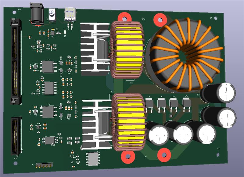
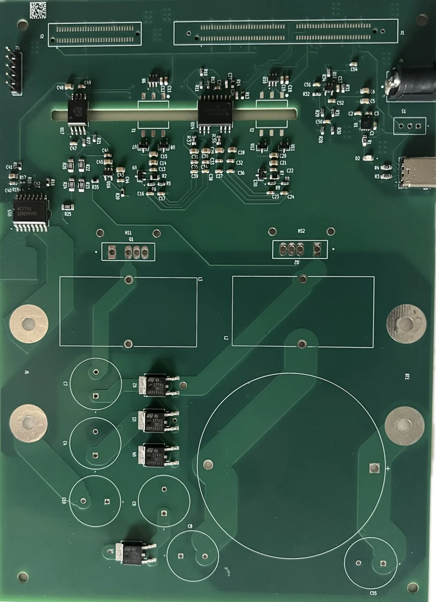
- Designed the PCB with switching frequencies up to approximately 50 kHz in mind.
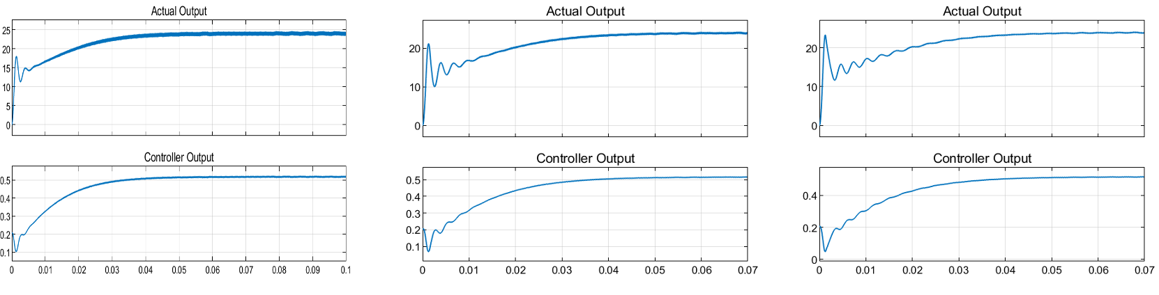
- Developed the closed-loop DC-link/output-voltage controller from small-signal converter behavior.
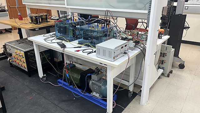
- Prepared the hardware platform for laboratory validation and iterative controller tuning.
02 / Approach
Methods & diagrams
Converter Topology
Series-parallel switched-inductor stages provide a high step-up ratio while keeping the architecture modular and scalable.
Power-Stage & PCB Design
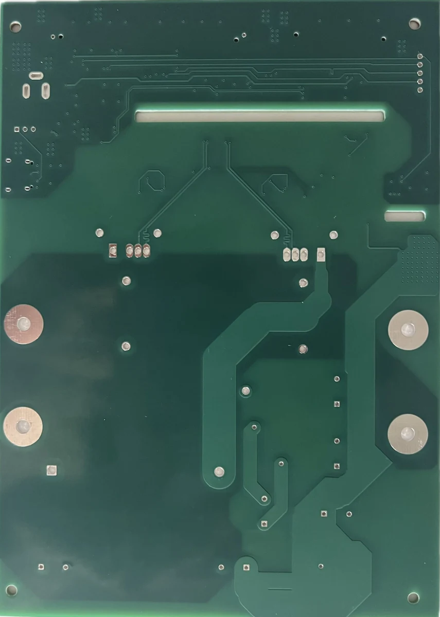
The electrical design was translated into a manufacturable PCB, including component placement, high-current paths, switching nodes, sensing, and control interfaces.
Closed-Loop Regulation
A feedback controller was designed from the converter small-signal dynamics to regulate the high-voltage DC output across operating conditions.
03 / Evidence
Results & gallery
Project figures and laboratory photographs. Open a figure to inspect the detail; vector PDFs are available for the control diagrams.
Findings
- The documented work includes a scalable switched-inductor topology, a 1 kW-class PCB design, and small-signal-based closed-loop voltage control.
Scope & limitations
The material documents topology development, PCB design, and prototype work. The 1 kW value denotes the design target; a complete measured efficiency map is not presented.